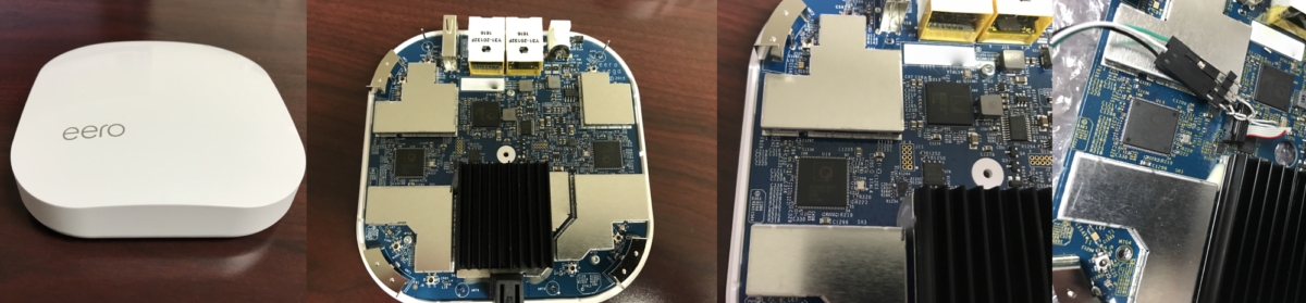
So far, I haven’t found any software ‘backdoors’ to gain access to the eero. So, for now, I’m getting in via hardware methods. This includes connecting to the serial port and the SPI flash chip (where the eero boots from). Thanks to my friend Al S. for the soldering help!
Here’s a photo of the eero main board:
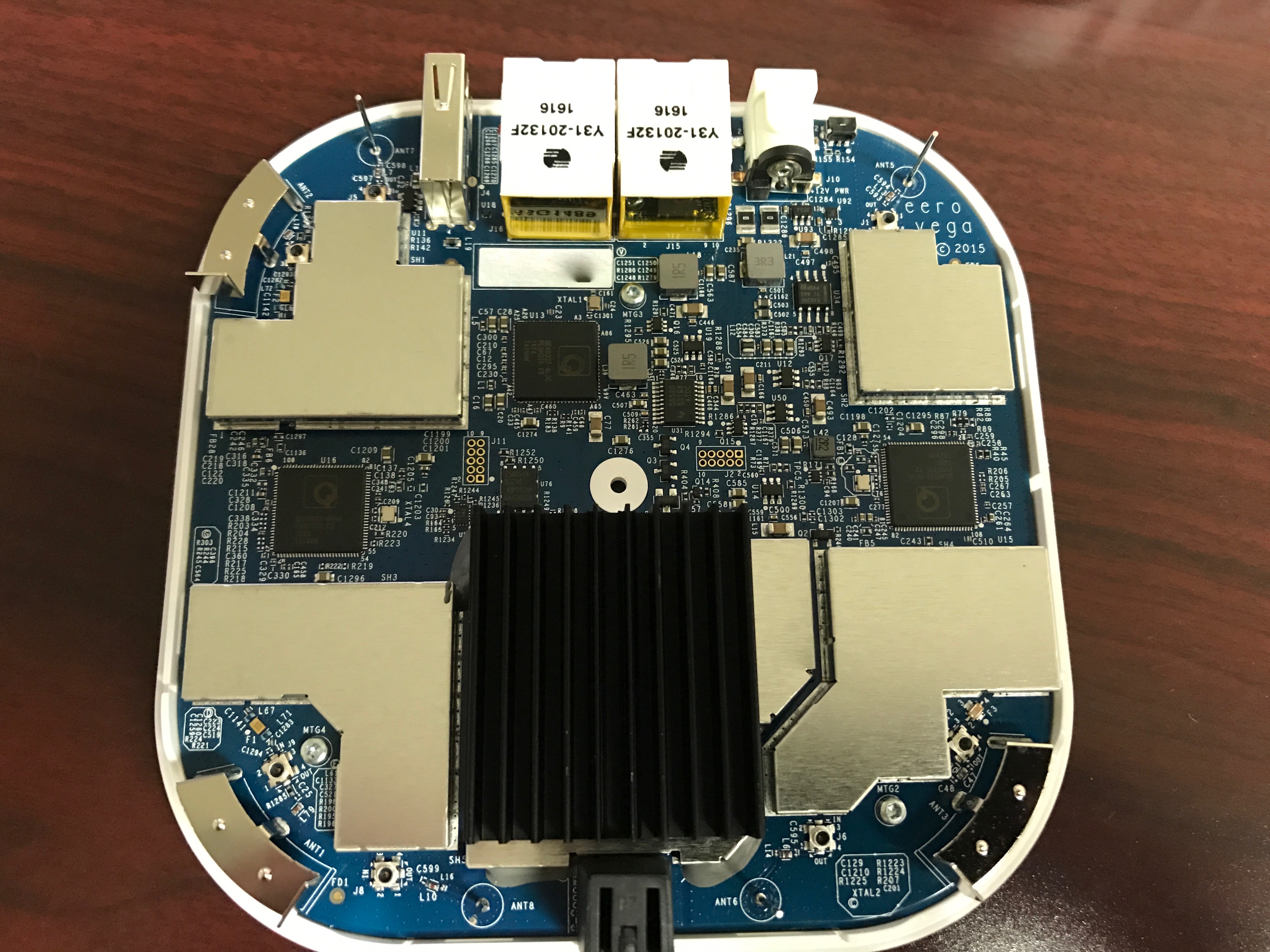
As you can see, there are two obvious ‘ports’ on the board (10-pin headers): J11 in the center/left (vertically oriented), and J2 in the center/right (horizontally oriented).
J11 seems to be a debug/manufacturing access port. It has the TTL-level serial port signals, as well as signals that connect to the SPI flash chip (the primary boot device, which includes the u-boot boot loader and other information).
I suspect that J2 is a JTAG port, but I really haven’t investigated it.
I have focused on J11 for my initial access to the hardware. Here is a close-up of the connector:
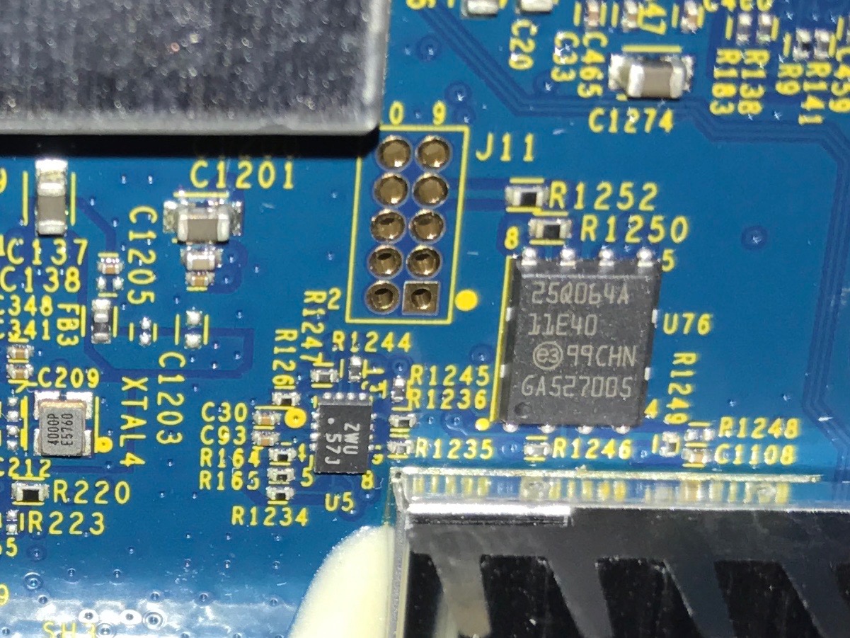
The SPI boot flash chip is just to the right of the J11 connector (25Q064A – datasheet). Another important chip (that I’ll get to later) is below J11 (marked ZWU 57J). This is TI SN74AVC4T245 bus level translation chip (datasheet).
I’ve buzzed-out the signals on the J11 connector – here’s a pinout:
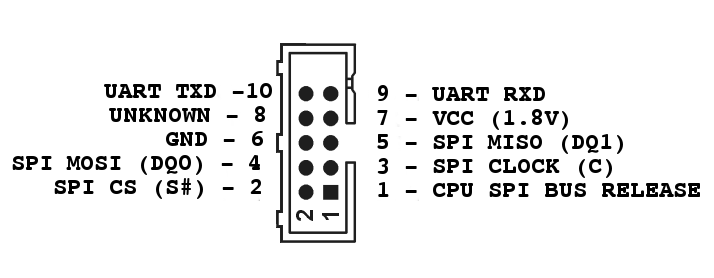
Serial port
It’s possible to get serial port access to the eero by connecting a TTL serial adapter to the UART TXD/RXD/GND signals on this connector.
Unfortunately, u-boot on the eero is configured with “bootdelay=0”, meaning it’s not possible to interrupt the boot process by typing control-C on the serial port. Also, by default, u-boot’s “bootargs” to the kernel leave the kernel’s console output going ‘nowhere’ (NOT to the serial port). So, by connecting to the serial port, you can only see the u-boot output, see it start the kernel, then you’ll see nothing else.
SPI flash
As described in the pinout above, the SPI flash signals are also brought-out to J11. Importantly, it’s possible to ‘disconnect’ the eero CPU from the SPI flash chip. This is necessary if you want to dump/reprogram the SPI flash chip – you don’t want the CPU doing accesses to the chip while you are.
This is where the “TI SN74AVC4T245” chip comes in. It’s a bus level translator. But, it also has ‘output enable’ signals that let you control the output signals from this chip (the ones that go from the CPU to the SPI flash chip).
By default, these output enable signals are ‘low’ (enabled). By pulling them ‘high’, the SPI flash signals from the CPU are disconnected from the SPI flash chip – leaving the SPI flash chip 100% accessible via the J11 port.
The CPU’s SPI chip-select (S#), SPI clock (C), and MOSI (DQ0) signals go through this bus level translator chip to the SPI flash chip. They are disconnected from the SPI flash chip when the output enable signals are pulled high.
Pin 1 on J11 connects to both of the output enable signals (pins 1 and 16) on the “TI SN74AVC4T245” chip. So, pulling pin 1 on J11 high will disconnect the CPU from the SPI flash chip. I’ve labelled pin 1 “CPU SPI BUS RELEASE” in the diagram above.
All of the other important SPI flash signals are brought to J11. So, it’s possible to connect an SPI flash programmer to J11, read the flash chip image, modify it, and write it back.
Reprogramming SPI flash to gain serial port access
I mentioned above that the u-boot image in the SPI flash has the environment variable “bootdelay” set to “0”, which prevents interruption of the boot process (by hitting control-C on the serial port, for example).
I gained access by reading the contents of the SPI flash chip to a file on my PC, modifying it to set “bootdelay” to “9”, then writing it back.
As you are editing the u-boot binary, if you search for “bootdelay=0”, you’ll see several occurrences. The initial ones are the ‘default’ environment variables that u-boot uses if it can’t find a valid environment in the SPI flash.
Later, there are two copies of the environment in flash (starting at offsets 0x002a0000 and 0x002b0000 – a primary and a redundant copy). NOTE that if you modify the “bootdelay=0” to “bootdelay=9” in these regions, you’ll need to update the 32-bit CRC at the start of the region (otherwise the environment will be considered ‘invalid’ and u-boot will revert to the ‘default’ compiled-in environment found earlier in the image).
After editing/writing the image back to SPI flash, you’ll be able to interrupt the boot process (by pressing control-C at the serial console).
Once you’ve interrupted the u-boot boot process, you can modify the “bootargs” environment variable to tell the Linux kernel to enable the serial port (add “console=ttyMSM0,115200n8 earlyprintk” to the existing kernel command line).
If you are interested, I used the “MiniPRO” TL866 universal programmer to reprogram my eero’s SPI flash. Here’s a photo of the programmer with the cable I used to connect to my eero’s J11 port:
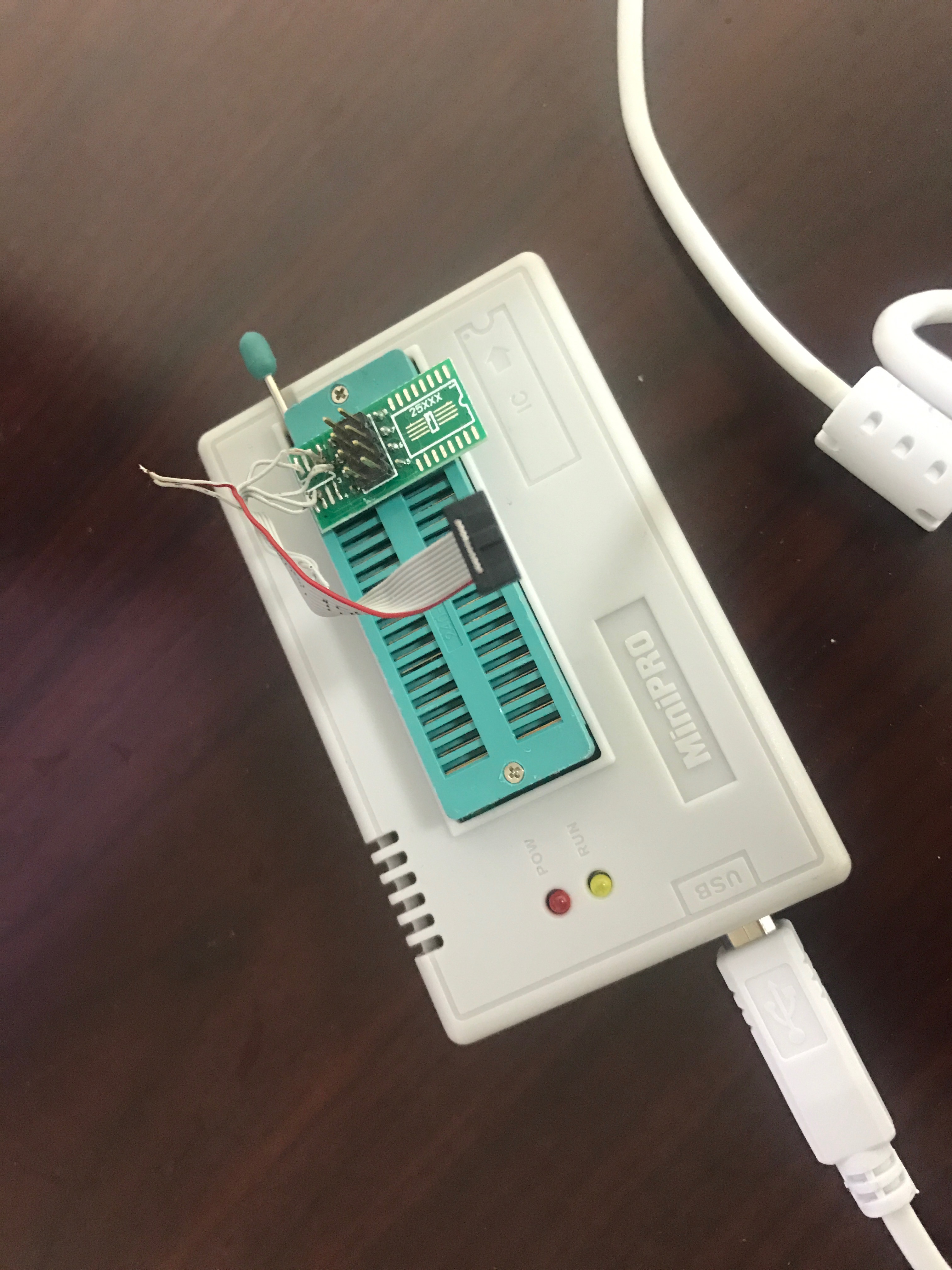
You’ll see signals from the cable connecting to the SPI flash pins on the ZIF adapter board that came with the programmer. You’ll also see a pair of floating wires connected to each other. Those are pins 1 (“CPU SPI BUS RELEASE”) and 7 (“VCC 1.8V”). Tying these two signals together pulls the output enable signals on the SN74AVC4T245 ‘high’ – disconnecting the CPU from the SPI flash chip (so it doesn’t interfere with our reading/writing to the flash chip).
Well done!